Veljko Milutinovic
Surviving the Design
of an MIMD Multimicroprocessor for DFT:
Lessons Learned
MULTIMICROPROCESSOR HF MODEM
FOR DSM RADIO
Origin and Environment:
Presentation and Education:
References:
[Milutinovic79] Milutinovic, V.,
A MOS Microprocessor-Based Medium-Speed Data Modem,"
Microprocessing and Microprogramming, March 1979, pp. 100–103.
[Milutinovic80] Milutinovic, V., Paunovic, R., Nedic, S., Jeftovic, M.,
"One Approach to Multimicroprocessor Implementation of a Modem
for Data Transmission over HF Radio,"
Proceedings of the Euromicro-80 Symposium,
London, England, UK, September 1980, pp. 107–111.
[Milutinovic85] Milutinovic, V.,
"A 4800 bit/s Microprocessor-Based CCITT Compatible Data Modem,"
Microprocessing and Microprogramming, February 1985, pp. 57–74.
[Milutinovic86] Milutinovic, V. Fortes, J., Jamieson, L.,
"A Multimicroprocessor Architecture for Real-Time Computation
of a Class of DFT Algorithms,"
IEEE Transactions on ASSP, October 1986, pp. 1301–1309.
LOW SPEED
SINGLE PROCESSOR DESIGN
Part#1: Low Speed Transmitter
|
Dibit |
00 |
01 |
11 |
10 |
|
dP |
0° |
+ 90° |
+ 180° |
+ 270° |
Figure X1: Correspondence between dibit values and phase changes (source: [Milutinovic78]).
Legend:
dP—phase difference.
a)
b)
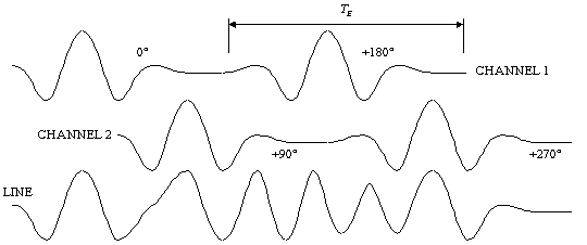
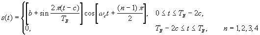
Figure X2: Line signal, a) formula, b) waveform (source: [Milutinovic78]).
Legend:
TE—envelope interval.
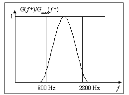
Figure X3: Line signal spectrum (source: [Milutinovic78]).
Legend:
f—frequency,
G(f +)/Gmax(f +)—normalized signal spectrum.
|
P0 = 0° |
P0 = + 90° |
||||
|
0.000 |
= |
00000000 |
0.000 |
= |
00000000 |
|
10.461 |
= |
00001010 |
–25.223 |
= |
11100111 |
|
–42.045 |
= |
11010110 |
–42.124 |
= |
11010110 |
|
–84.793 |
= |
10101011 |
34.983 |
= |
00100011 |
|
–0.223 |
= |
00000000 |
119.032 |
= |
01110111 |
|
126.704 |
= |
01111111 |
52.832 |
= |
00110101 |
|
101.886 |
= |
01100110 |
–101.314 |
= |
10011011 |
|
–52.117 |
= |
11001100 |
–127.000 |
= |
10000001 |
|
–119.031 |
= |
10001001 |
–0.447 |
= |
00000000 |
|
–35.460 |
= |
11011101 |
84.595 |
= |
01010101 |
|
41.886 |
= |
00101010 |
42.281 |
= |
00101010 |
|
25.281 |
= |
00011001 |
–10.319 |
= |
11110110 |
|
0.000 |
= |
00000000 |
0.000 |
= |
00000000 |
|
0.000 |
= |
00000000 |
0.000 |
= |
00000000 |
|
0.000 |
= |
00000000 |
0.000 |
= |
00000000 |
|
0.000 |
= |
00000000 |
0.000 |
= |
00000000 |
|
P0 = + 180° |
P0 = + 270° |
||||
|
0.000 |
= |
00000000 |
0.000 |
= |
00000000 |
|
–10.461 |
= |
11110110 |
25.223 |
= |
00011001 |
|
42.045 |
= |
00101010 |
42.124 |
= |
00101010 |
|
84.793 |
= |
01010100 |
–34.983 |
= |
11011101 |
|
0.223 |
= |
00000000 |
–119.032 |
= |
10001001 |
|
–126.704 |
= |
10000001 |
–52.832 |
= |
11001011 |
|
–101.886 |
= |
10011001 |
101.314 |
= |
01100101 |
|
52.117 |
= |
00110100 |
127.000 |
= |
01111111 |
|
119.031 |
= |
01110111 |
0.447 |
= |
00000000 |
|
35.460 |
= |
00100011 |
–84.595 |
= |
10101011 |
|
–41.886 |
= |
11010110 |
–42.281 |
= |
11010110 |
|
–25.281 |
= |
11100111 |
10.319 |
= |
00001010 |
|
0.000 |
= |
00000000 |
0.000 |
= |
00000000 |
|
0.000 |
= |
00000000 |
0.000 |
= |
00000000 |
|
0.000 |
= |
00000000 |
0.000 |
= |
00000000 |
|
0.000 |
= |
00000000 |
0.000 |
= |
00000000 |
Figure X4: Line signal samples (source: [Milutinovic78]).
Legend:
P0—initial phase.
Part#2: Low Speed Receiver (Suboptimal Detection)
According to [Helstrom68],
the probability of correct detection (Qd) of the phase (
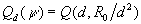
where d2 and R0 are SNR and phase decision threshold, respectively.
Provided the above conditions are satisfied,
the impulse responses h(t) of 4 filters matched to the signals
s(t;
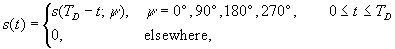
TD
corresponds to dibit rate.Figure X5: Theoretical foundations of statistical signal detection (source: [Milutinovic78]).
Legend:
y
—signal phase,s(t, y )—signal which is to be detected.
|
P0 |
Signs |
|
0° |
+ + + + |
|
+ 90° |
+ + - - |
|
+ 180° |
- - - - |
|
+ 270° |
- - + + |
Figure X6: Correspondence between sample signs and initial phase of the line signal
(source: [Milutinovic78]).
Legend:
P0—initial phase.
Optimum sampling instants are given by the abscissa of local maxima of the following function:
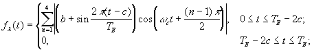
Figure X7: Optimum sampling instants for maximal signal to noise ratio
(source: [Milutinovic78]).
Legend:
TE—envelope interval.
References:
[Helstrom68] Helstrom, G.,
Statistical Theory of Signal Detection,
Pergamon Press, Oxford, England, 1968.
[Milutinovic80a] Milutinovic, V.,
"Suboptimum Detection Procedure Based in the Weighting of Partial Decisions,"
IEE Electronic Letters, Vol. 16, No. 6, 13th March, 1980, pp. 237–238.
[Milutinovic80b] Milutinovic, V.,
"Comparison of Three Suboptimum Detection Procedures,"
IEE Electronic Letters, Vol. 16, No. 17, 14th August 1980, pp. 683–685.
[Milutinovic84] Milutinovic, V.,
"Performance Comparison of Three Suboptimum Detection Procedures
in Real Environment,"
IEE Proceedings Part F, Vol. 131, No. 4, July 1984, pp. 341–344.
[Milutinovic85] Milutinovic, V.,
"Generalized W.P.D. Procedure for Microprocessor Based Signal Detection,"
IEE Proceedings Part F, Vol. 132, No. 1, February 1985, pp. 27–35.
[Milutinovic88] Milutinovic, V.,
"A Comparison of Suboptimal Detection Algorithms
Applied to the Additive Mix of Orthogonal Sinusoidal Signals,"
IEEE Transactions on Communications, Vol. COM-36, No. 5, May 1988,
pp. 538–543.
Figure X8: Maximum likelihood function with noise (source: [Milutinovic78]).
Legend:
TE—envelope interval.
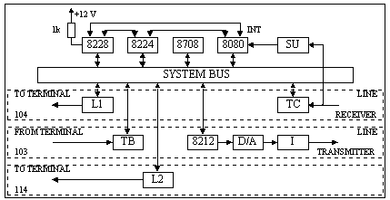
Figure X9: System structure (source: [Milutinovic78]).
Legend:
SU—synchronization unit,
L1/2—latches,
TB/C—tristate buffers,
I—interpolator.
MEDIUM SPEED
SINGLE PROCESSOR DESIGN
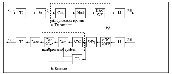
Figure X10: Structure of a 4800 b/s CCITT compatible modem (source: [Milutinovic78]).
Legend:
TI—terminal interface,
Sc—scrambler,
Cod—coder,
Mod—modulator,
DAC—digital to analog converter,
IF—interpolating filter,
LI—line interface,
AGC—automatic gain control,
BPF—band pass filter,
StEq—statistical equalizer,
ADC—analog to digital converter,
Dem—demodulator,
Det&Dec—detector and decoder,
TE—timing extractor,
Desc—descrambler,
{ai}—input data stream,
{bi}—scrambled data stream,
S[t]—line signal.
Part#1: Medium Speed Transmitter
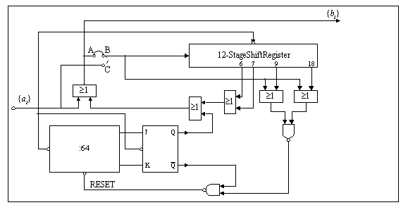
Figure X11: Scrambler Structure (source: [Milutinovic78]).
Legend:
 —generating polynomial with additional guard
against repeating patterns of 1, 2, 3, 4, 6, 9, and 12 bits,
{ai}—input data stream,
{bi}—output data stream,
Note: if strap BC is used instead of strap AB,
the scrambler turns into the descrambler; the clock input is implied.
|
Tribit values |
Phase values |
||
|
0 |
0 |
1 |
0° |
|
0 |
0 |
0 |
45° |
|
0 |
1 |
0 |
90° |
|
0 |
1 |
1 |
135° |
|
1 |
1 |
1 |
180° |
|
1 |
1 |
0 |
225° |
|
1 |
0 |
0 |
270° |
|
1 |
0 |
1 |
315° |
Figure X12: The CCITT V.27 coding scheme implemented in the modem under consideration
(source: [Milutinovic78]).
Legend: Self-explanatory.
The left–hand digit of the tribit is the one occurring first in the data stream.
The phase change is the actual on–line phase shift in the transition region
from the center of one signaling element to the center of the following signaling element.
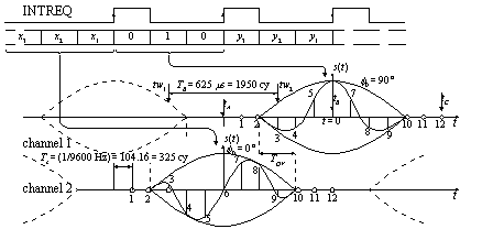
Figure X13: Two components making the line signal (source: [Milutinovic78]).
Legend:
f
0—initial phase of the signal, in the center of the signaling interval,Ts—sampling period in the transmitter,
TA—envelope interval,
TOV—overlapping interval (of two consecutive symbols),
Tc—carrier period,
TB—signaling interval,
cy—basic cycle of the microprocessor system,
X1—the first occurring bit of the tribit X3X2X1
(in this example, it is causing the appearance of the line symbol with f 0 = 0° ),
010—the tribit occurring as the next to X3X2X1 in the stream
(in this example, it is causing the appearance of the line symbol with f 0 = 90° ),
INTREQ—signal on the microprocessor pin INT,
tA, tB, tC—interrupt request instants (in the transmitter),
tw1, tw2—signaling limits (interrupt request instants in the receiver).
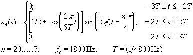
The analytical expression for the signal on the envelope interval can have only 8 different forms. There are 12 samples in total, on condition that the 9.6 kHz sampling frequency is chosen.
The values of these samples (8 groups with 12 samples in each group) normalized
with the constant 127 are given by the following expression:
Figure X14: Analysis of the line signal (source: [Milutinovic78]).
Legend: Self-explanatory.
|
|
00FFH |
|
111 ® D f =180° |
01FFH |
|
|
02FFH |
|
|
03FFH |
||
|
|
|
|
B8 |
01E0H |
|
|
|
|
315 ° |
03E0H |
||
|
|
|
|
110 ® D f =225° |
|
|
|
|
|
|
|
||
|
|
|
|
B7 |
01C0H |
|
|
|
|
270 ° |
03C0H |
||
|
|
|
|
101 ® D f =315° |
|
|
|
|
|
|
|
||
|
|
|
|
B6 |
01A0H |
|
|
|
|
225 ° |
03A0H |
||
|
|
|
|
100 ® D f =270° |
|
|
|
|
|
|
|
||
|
|
|
|
B5 |
0180H |
|
|
|
|
180 ° |
0380H |
||
|
|
|
|
011 ® D f =135° |
|
|
|
|
|
|
|
||
|
|
|
|
B4 |
0160H |
|
|
|
|
135 ° |
0360H |
||
|
|
|
|
010 ® D f =90° |
|
|
|
|
|
|
|
||
|
|
|
|
B3 |
0140H |
|
|
|
|
90 ° |
0340H |
||
|
A |
0038H |
|
001 ® D f =45° |
|
|
|
|
|
|
|
||
|
|
|
|
B2 |
0120H |
|
|
|
|
45 ° |
0320H |
||
|
|
|
|
000 ® D f =0° |
|
|
|
|
|
|
|
||
|
INIC |
0000H |
|
B1 |
0100H |
|
C |
0200H |
|
0 ° |
0300H |
||
|
1444444444444442444444444444443 ProgramMemory |
|
144424443 DataMemory |
||||||||||
Figure X15: Memory organization of the transmitter design (source: [Milutinovic78]).
Legend:
 —memory occupied by code (program or data),
 —free memory space,
ProgramMemory—memory space occupied by program code,
DataMemory—memory space occupied by data code,
Page No. 0—memory page with initialization routines,
Page No. 1—memory page with the precoding routine,
Page No. 2—memory page with the signal forming routine,
Page No. 3—memory page with 8 possible groups of signal samples
(existing on the envelope interval).
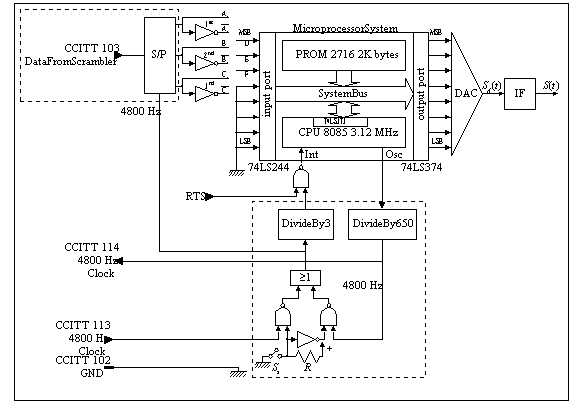
Figure X16: Transmitter structure (source: [Milutinovic78]).
Legend:
MSB—the most significant bit,
LSB—the least significant bit,
RTS—request-to-send,
S(t)—line signal,
SA(t)—zero-order polynomial-based approximation of the line signal,
T—bit interval,
Ss—synchronization switch (Ss = ON: modem master; Ss = OFF: terminal master),
S/P—serial-to-parallel converter,
IF—second-order low-pass filter as interpolating filter,
DAC—eight-bit digital-to-analog converter,
R—appropriate resistor.
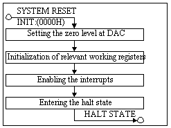
Figure X17: Flow chart of the transmitter initialization code. (source: [Milutinovic78]).
Legend:
DAC—Digital-to-Analog Converter.
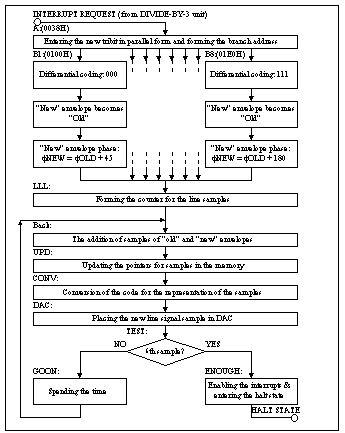
Figure X18: Flow chart of the transmitter operation code (source: [Milutinovic78]).
Legend:
DAC—Digital-to-Analog Converter.
Part#1: Medium Speed Receiver (Optimal Detection)
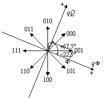
Figure X19: Symbolics of the detection process (source: [Milutinovic78]).
Legend:
qF —previous signal in "quasiphase,"
qQ—previous signal in "quasiquadrature,"
F
—inphase projection of current signal,Q—quadrature projection of current signal,
sign Q—first bit to occur at the receiver output,
sign F —second bit to occur at the receiver output,
logical value of  —third bit to occur at the receiver output,
TRUE ® bit 1,
FALSE ® bit 0.
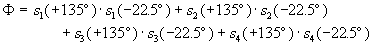
After the formation of quantities
F and Q, is false, or bit ‘1’ if is true.
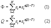
Figure X20: Mathematics of the detection process (source: [Milutinovic78]).
Legend:
N—number of samples (N = 4),
si (i = 1, …, N)—signal samples from the current signaling interval,
si qF F(- T) (i = 1, …, N)—signal samples from the previous signaling interval
(after the - 22.5° phase shifter),
siqQ(- T) (i = 1, …, N)—signal samples from the previous signaling interval
(after the + 67.5° phase shifter).
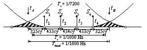
Figure X21: Clocking of the detection process (source: [Milutinovic78]).
Legend:
Tc—carrier period,
Tbaud—Baud period,
Ts—sampling period,
tA, tB—symbol limits,
t1, t2, t3, t4—nominal sampling instants.
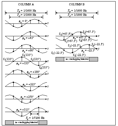
Figure X22: Sampling of the detection process (source: [Milutinovic78]).
Legend:
—overlapping interval,
—overlapping-free interval (when envelope shaping is present),
Column A—direct signal with different initial phases,
Column B—direct signal with j = 0 after propagation through phase shifters,
TS—sampling period,
TB—signaling interval,
TC—carrier period.
During the demodulation procedure it is necessary to calculate the following:
(3)
(4)
Taking the specific case into account, the following is obtained:

(5)

(6)
So, if sign Q = 0 is sent to the terminal first, sign
F = 1 second, and bit ‘1’ (since ) last, the receiver output will correspond to the transmitter input, i.e. tribit 011.
Figure X23: Numerics of the detection process (source: [Milutinovic78]).
Legend: Self-explanatory.
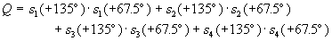
Figure X24: Hardware for the detection process (source: [Milutinovic78]).
Legend:
P1, P2, P3—input ports,
P4—output port,
M1, M2—multiplier inputs,
M3—high-order byte of the multiplier output,
S&H—sample-and-hold circuit,
AD—analog-to-digital converter,
CL—control logic generating support signals for S&H and AD,
—chip-select signal for port P1,
F
2TTL—basic microprocessor clock: 3.12 MHz,S/ —control signal for S&H circuits,
SOC—control signal for ADs,
MSB—the most significant bit,
P/S—parallel-to-serial converter,
PhSh—analog phase-shift circuit,
A, B, C, D, E, F—straps for matching the coding scheme of the receiver to that of the transmitter; nominal strap configuration AD + BE + CF,
NOTE: the propagation time through all phase-shift circuits must be the same.
|
|
03FFH |
|
ADR(PORT1) |
=E462H |
|
|
|
|
|
|
|
|
ADR(PORT2) |
=E463H |
|
5400, 5401 |
5408, 5409 |
S 1 |
|
|
|
|
ADR(PORT3) |
=E464H |
|
5402, 5403 |
540A, 540B |
S 2 |
|
|
|
|
ADR(PORT4) |
=E465H |
|
5404, 5405 |
540C, 540D |
S 3 |
|
|
|
|
ADR(M1) |
=E463H |
|
5406, 5407 |
540E, 540F |
S 4 |
|
|
|
|
ADR(M2) |
=E464H |
|
14243 |
14243 |
|
|
|
|
|
ADR(M3) |
=E465H |
|
Previous |
Current |
|
|
|
|
|
|
|
|
BaudInterval |
BaudInterval |
|
|
|
|
|
– – – – – – – – |
[54E4H] = F + |
|
14444244443 |
|
|
|
|
|
|
– – – – – – – – |
[5465H] = Q - |
|
Samples from the |
|
|
|
|
|
|
– – – – – – – – |
[5458H] = F - |
|
"quasiphase" and |
|
|
|
|
|
|
– – – – – – – – |
[5454H] = Q + |
|
"quasiquadrature" channel |
|
|
|
REC |
0038H |
|
|
540FH |
|
in the memory |
|
|
|
|
|
|
|
M |
|
region: SAMP |
|
|
|
|
|
|
SAMP |
5400H |
|
|
|
|
|
INIC |
0000H |
|
|
|
|
|
|
|
Figure X25: Memory organization of the receiver design (source: [Milutinovic78]).
Legend:
INIC—initialization routine,
REC—main program in the receiver,
SAMP—memory space for "old" and "new" envelope samples,
qQ(Si)—symbolical memory address of the i-th sample from the "quasiquadrature" channel; (i = 1, …, 4),
qF (Si)—symbolical memory address of the i-th sample from the "quasiphase" channel; (i = 1, …, 4).
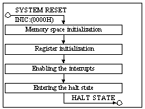
Figure X26: Flow chart of the receiver initialization code (source: [Milutinovic78]).
Legend: Self-explanatory.
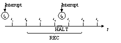
Figure X27: Timing of the receiver code (source: [Milutinovic78]).
Legend:
REC—time interval covered by the main program in the receiver,
HALT—time interval when the processor is in the halt state,
ta, tb—limits of the signaling interval,
t1, t2, t3, t4—sampling instants.
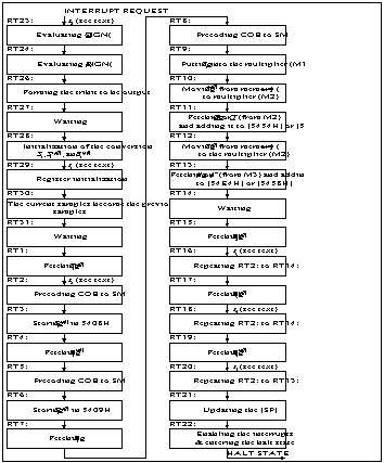
Figure X28: Flow chart of the receiver operation code (source: [Milutinovic78]).
Legend:
SM—Signed Magnitude,
COB—Complementary Offset Binary.
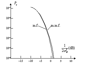
Figure X29: Impact of the Gaussian noise (source: [Milutinovic78]).
Legend:
m.f.—optimum matched filter,
m.m.f.—modified matched filter, i.e., the approach under consideration here,
Pe —probability of error,
s
B—variance of the bandlimited Gaussian noise.
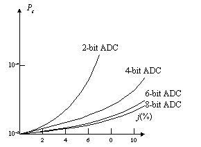
Figure X30: Impact of the quantization noise (source: [Milutinovic78]).
Legend:
Pe —error probability,
j—jitter in percent of the signaling interval time,
ADC—analog-to-digital converter.
MEDIUM SPEED
MULTIPLE PROCESSOR DESIGN
During a single signaling interval lasting T = 13.33 ms, composite signal is given by:

Symbols  , and
, and  ,
,
refer to subchannel carrier frequency and its initial phase, respectively.
After being corrupted by multiplicative and additive disturbances,
the signal received is decomposed on the basis of mutual orthogonality of subsignals
over the middle T0 portion of the signaling interval.
The frame is reconstructed according to the signs of
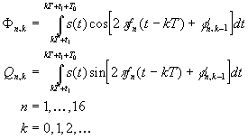
Here t1 being related to the beginning of the signaling interval. In the case of digital realization, with the samples s(tj), j = 0, 1, 2, … being 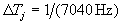 apart, it is:
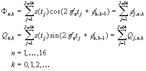
Finally, the phase difference between the received signal carrier (
f n,k)Figure X31: Mathematics of the HF data modem signal forming and detection
(source: [Milutinovic78]).
Legend: Self-explanatory.
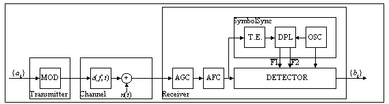
Figure X32: Structure of the receiver (source: [Milutinovic78]).
Legend:
{ak} transmitting bit stream k = 0, 1, …,
{bk} receiving bit stream k = 0, 1, …,
C( f, t) fading channel transfer function,
n(t) additive noise,
T.E. timing extraction,
DPL digital phase locking,
OSC crystal oscillator,
AGC automatic gain control,
AFC Doppler effect correction,
75 Hz clock with phase locked to the incoming signal frame transitions,
2400 Hz clock synchronized with .
Part#1: Medium Speed Transmitter
Part#2: Medium Speed Receiver (Optimal Detection)
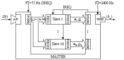
Figure X33: Structure of the detector (source: [Milutinovic78]).
Legend:
PO—output port,
PI—input port.

Figure X34: The detection formula (source: [Milutinovic78]).
Legend: Self-explanatory.
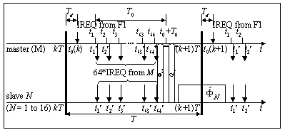
Figure X35: Timing of the receiver code (source: [Milutinovic78]).
Legend: Self-explanatory.
|
L [%] |
Qv & F v |
Qw & F w |
|
25 |
10 |
10 |
|
50 |
9 |
9 |
|
75 |
9 |
9 |
|
100 |
8 |
8 |
Figure X36: Number of bits required in representation of final F n,k and Qn,k
for various values of the limitation factor L (source: [Milutinovic78]).
Legend: Self-explanatory.